“TSMC-UTokyo Lab” Launched to Promote Advanced Semiconductor Research, Education and Talent Incubation

The University of Tokyo (UTokyo) and TSMC announced the opening of the “TSMC-UTokyo Lab” this June, dedicated to advancing semiconductor research, education and talent incubation. As TSMC’s first joint lab with a university outside Taiwan, it will leverage the extensive knowledge, experience, and creativity of these two global leaders in their fields. Together, TSMC and UTokyo aim to promote cutting-edge research and development in semiconductor technologies, generate innovative solutions, and cultivate semiconductor talent, all while working towards a shared vision of “creating and advancing sustainable semiconductor technologies for the next generation and contributing to society”.


Since 2019, UTokyo and TSMC have collaborated at both the university and company-wide level on leading-edge semiconductor research, leading to 21 research projects which have achieved fruitful research results. Furthermore, TSMC and UTokyo have extended their industry–academia partnership to include semiconductor education and next-generation talent incubation. In 2023, UTokyo adopted the “TSMC N16 (FinFET) ADFP*1”, specialized for advanced process design education and the first of its kind at a Japanese university, into courses at its Faculty of Engineering and Graduate School of Engineering. To further collaborate more systematically and strategically, UTokyo and TSMC signed the “Strategic Industrial/Academic Collaboration Agreement” taking effect in April this year to promote research, education, and talent development. In addition to the establishment of the TSMC-UTokyo Lab, the “Social Cooperation Program” was launched in UTokyo in line with specific initiatives set out in the agreement.

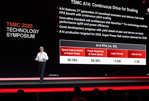
Located on UTokyo’s Asano campus in the Hongo district, the Lab will be managed by UTokyo faculty and staff guided by directors from both UTokyo and TSMC, serving as a central hub for a Strategic Collaboration initiative. The Lab will facilitate research in semiconductor technologies with an emphasis on practical applications in the future, covering areas such as materials, devices, processes, metrology, packaging, and circuit design. Research findings will not only be applied to TSMC’s R&D and chip manufacturing but will also be shared regularly at a technology symposium held at UTokyo. Since 2019, these symposiums have provided a platform for UTokyo faculty and students to engage with TSMC R&D staff. Additionally, the Lab will explore collaboration through activities such as TSMC-sponsored project calls and internship opportunities.

“In an era where challenges and rapid changes surround humanity and the future is hard to foresee, universities should not only refine their knowledge in diverse fields but also collaborate with different sectors beyond academia to contribute to solving global challenges and to nurture the talent who will shape the future,” said Teruo Fujii, President of UTokyo. “Through our collaboration with TSMC, we aim to pursue broad social implementation and actively engage with the historic challenges that humanity shares.”

“The TSMC–UTokyo Lab is built on the success of institution-wide collaboration that started in 2019, which has blossomed into the close collaboration that we have today,” said Dr. Y.J. Mii, Executive Vice President and Co-Chief Operating Officer at TSMC. “TSMC and UTokyo are both global leaders in their respective fields, and we hope that this lab will serve as a hub for a broad and long-lasting partnership to expand the boundaries of knowledge in the field of semiconductors and nurture generations of talent for the future.”

In addition to deepening research efforts, through this partnership UTokyo will offer the most comprehensive infrastructure for advanced semiconductor design education and hands-on research opportunities, cultivating talent poised to lead in the global semiconductor arena. TSMC, along with its Japan Design Center, Japan 3DIC R&D Center, and Japan Advanced Semiconductor Manufacturing (JASM) specialty fab, will leverage the Lab to further its next-generation talent development. Positioning the Lab as a focus point for semiconductor research in Japan, UTokyo and TSMC will collaborate towards the goal of nurturing domestic talent and advancing the creation and development of sustainable next-generation semiconductor technologies to positively impact society.

TSMC Unveils Next-Generation A14 Process at North America Technology Symposium

TSMC unveiled its next cutting-edge logic process technology, A14, at the Company’s North America Technology Symposium this April. Representing a significant advancement from TSMC’s industry-leading N2 process, A14 is designed to drive AI transformation forward by delivering faster computing and greater power efficiency. It is also expected to enhance smartphones by improving their on-board AI capabilities, making them even smarter. Planned to enter production in 2028, the current A14 development is progressing smoothly with yield performance ahead of schedule.


Compared with the N2 process, which is about to enter volume production later this year, A14 will offer up to 15% speed improvement at the same power, or up to 30% power reduction at the same speed, along with more than 20% increase in logic density. Leveraging the Company’s experience in design-technology co-optimization for nanosheet transistor, TSMC is also evolving its TSMC NanoFlex™ standard cell architecture to NanoFlex™ Pro, enabling greater performance, power efficiency and design flexibility.

“Our customers constantly look to the future, and TSMC’s technology leadership and manufacturing excellence provides them with a dependable roadmap for their innovations,” said TSMC Chairman and CEO Dr. C.C. Wei. “TSMC’s cutting-edge logic technologies like A14 are part of a comprehensive suite of solutions that connect the physical and digital worlds to unleash our customers’ innovation for advancing the AI future.”

In addition to A14, TSMC also debuted new logic, specialty, advanced packaging and 3D chip stacking technologies, each contributing to broad technology platforms in High Performance Computing (HPC), Smartphone, Automotive, and Internet of Things (IoT). These offerings are designed to equip customers with a comprehensive suite of interconnected technologies to drive their product innovations. They include:

High Performance Computing

TSMC continues to advance its Chip on Wafer on Substrate (CoWoS®) technology to address AI’s insatiable need for more logic and high-bandwidth memory (HBM). The company plans to bring 9.5 reticle size CoWoS to volume production in 2027, enabling integration of 12 HBM stacks or more in a package together with TSMC’s leading-edge logic technology. After showcasing its revolutionary System-on-Wafer (TSMC-SoW™) technology in 2024, TSMC followed up with SoW-X, a CoWoS-based offering to create a wafer-sized system with computing power 40X the current CoWoS solution. Volume production is scheduled for 2027.

TSMC offers a host of solutions to compliment the sheer computing power and efficiency of its logic technologies. These include silicon photonics integration with TSMC’s Compact Universal Photonic Engine (COUPE™), N12 and N3 logic base die for HBM4, and a new Integrated Voltage Regulator (IVR) for AI with 5X vertical power density delivery compared with a separate power management chip on the circuit board.

Smartphone

TSMC is supporting AI on edge devices and its need for high-speed, low-latency wireless connectivity to move massive data with N4C RF, the latest generation of TSMC’s radio frequency technology. N4C RF delivers 30% power and area reduction versus N6RF+, making it ideal for packing more digital content into RF system-on-chip designs to meet the requirements of emerging standards such as WiFi8 and AI-rich True Wireless Stereo. It is scheduled to enter risk production in first quarter of 2026.

Automotive

Advanced Driver Assistance Systems (ADAS) and Autonomous Vehicles (AV) pose stringent demands for computing power with no compromise on automotive-grade quality and reliability. TSMC is meeting customers’ needs with the most advanced N3A process going through the final stage of AEC-Q100 Grade-1 qualification, and continuous defect improvement to meet Automotive defective parts per million (DPPM) requirements. N3A is entering production for automotive applications, joining a full suite of technologies for future software-defined vehicles.

Internet of Things

As everyday electronics and appliances adopt AI functionality, IoT applications are taking on greater computational tasks while remaining on a slim budget for battery power. With TSMC’s previously announced ultra-low power N6e process now in production, the company is targeting N4e to continue pushing the envelope of power efficiency for future edge AIs.

TSMC’s North America Technology Symposium in Santa Clara, California, is the Company’s flagship customer event of the year, with more than 2,500 people registered to attend. At the symposium, TSMC not only updates customers on its latest technology developments, it also provides start-up customers with an “Innovation Zone” to showcase their unique products, as well as opportunities to pitch to potential investors. The North America symposium also kicks off a series of Technology Symposiums around the world in the coming months.

TSMC Commits to Ambitious Carbon Reduction Path in Line with Science Based Targets Initiative

TSMC marked Earth Day by announcing its commitment to the Science Based Targets Initiative (SBTi) this April, underscoring its dedication to addressing the pressing challenges of climate change. In line with SBTi, TSMC is collaborating with partners to achieve its environmental sustainability goals, embarking on an ambitious and comprehensive carbon reduction path encompassing direct, indirect and value chain emissions.


To drive sustainable growth, TSMC has outlined a blueprint for achieving net-zero emissions. Key milestones include peaking carbon emissions in 2025, reducing them to 2020 levels by 2030 with a target of using 60% renewable energy for global operations (RE60), achieving RE100 by 2040, and reaching net-zero emissions by 2050. Using 2025 as a baseline, TSMC commits to achieving absolute reduction targets for scope 1, 2, and 3 emissions aligned with the SBTi Corporate Net-Zero Standard within the next decade.

“Corporate engagement is one of the key drivers of change in the global pursuit of environmental commitments and low-carbon transformation,” stated Dr. C.C. Wei, TSMC Chairman and CEO, and ESG Steering Committee Chairman. “TSMC works closely with our supply chain partners and stakeholders to advance green initiatives and develop innovative energy-saving and carbon reduction technologies to achieve net-zero emissions. We are committed to setting ambitious goals and taking action to strive for a sustainable future.”

TSMC actively reduces Scope 1 direct greenhouse gas emissions by updating and installing local scrubbers and utilizing carbon-neutral natural gas. As of April, TSMC has earned its 53rd LEED (Leadership in Energy and Environmental Design) Gold or higher certification, making it the semiconductor industry leader in certified building area. TSMC's overseas operations have achieved net-zero emissions for Scopes 1 and 2 since 2022.

To address Scope 2 indirect energy emissions, TSMC became the first semiconductor company to join the global RE100 initiative for 100% renewable energy consumption. In 2023, TSMC accelerated its RE100 timeline, moving the target from 2050 to 2040, while expanding renewable energy usage and diversifying supply sources. The Company’s renewable energy usage surpassed 14% in 2024, while consistently achieving 100% renewable energy consumption across global offices and oversea sites, steadily progressing towards the RE60 medium-term target by 2030.

To reduce Scope 3 value chain emissions, TSMC pioneered an innovation model with a 20-year joint procurement agreement for 20,000 GWh of renewable energy, securing stable prices for suppliers and TSMC’s subsidiaries and lowering adoption barriers. In 2024, TSMC launched a supply chain carbon reduction subsidy project to fund local Tier-1 raw material suppliers in upgrading, replacing, or installing new equipment to enhance emission reduction efforts. This initiative aims to achieve an estimated reduction of 450,000 metric tons of carbon emissions—equivalent to the annual carbon sequestration capacity of 45,000 hectares of forest.

To accelerate the green transformation of the semiconductor supply chain, TSMC is partnering with major emission contributors to sign the TSMC Greenhouse Gas Reduction, Emissions Elimination & Neutrality (GREEN) Agreement for suppliers starting in 2025. Over 50 suppliers have signed, representing nearly 90% of TSMC's supply chain carbon emissions. The goal is to achieve RE85 for production in Taiwan and RE100 for overseas production of products supplied to TSMC by 2030. Additionally, aim for a carbon reduction target aligned with Science-Based Targets (SBT) initiatives by 2035.

TSMC offers industry-leading semiconductor process technology with superior performance and energy efficiency, enabling more efficient Information and Communication Technology (ICT) and smart applications. According Industrial Technology Research Institute's estimates, by 2030, every unit (kWh) of electricity TSMC uses in production for HPC-related semiconductor products can save 6.8 units globally, demonstrating the impact of TSMC's products and environmental value.

TSMC acts on its “ESG Policy” and “Environmental Protection Policy.” Guided by the principle of “beginning with the end in mind,” TSMC dynamically adjusts or sets more aggressive carbon reduction paths by annually reviewing target achievement, proactively addressing climate change challenges.

The SBTi is a global, collaborative effort that provides companies and organizations with a framework to set greenhouse gas emission reduction targets in line with the latest climate science. The initiative aims to help companies transition to a low-carbon economy by ensuring their targets are consistent with the level of decarbonization required to keep global temperature increase below 1.5°C or well below 2°C compared to pre-industrial levels, as outlined in the Paris Agreement.

Top