COVID-19 has fundamentally accelerated the digital transformation, making semiconductors more pervasive and essential in people’s lives. As communities start to reopen, we’re seeing opportunities brought by the multi-year megatrends of 5G and HPC-related applications that are expected to fuel massive increase in computation power and greater need for energy-efficient computing. With TSMC’s technology leadership, manufacturing excellence, and state-of-the-art design ecosystem, we will continue to help you unleash your silicon innovations and capture those growth opportunities in a new era of digitalization.
TSMC offers the foundry segment’s broadest technology portfolio and continues to invest in advanced technologies, specialty technologies, and advanced packaging and silicon stacking technologies, to provide customers more added value. TSMC’s N5 process is the foundry industry’s most advanced solution with the best PPA. Our N5 is already in its second year of volume production with yield well on track. To further enhance our 5nm family’s performance, power, and density improvements for next-wave 5nm products, TSMC introduced N4 technology, which is a straightforward migration from N5 with compatible design rules. Risk production of our N4 will begin this quarter with volume production scheduled for 2022. Our N3 process will be another full scaling from our N5 and will use FinFET transistor structure to deliver the best technology maturity, performance, and cost for our customers. Our 3nm technology will be the most advanced foundry technology in both PPA and transistor technology when it is introduced.
TSMC's mission is to be the trusted technology and capacity provider for the global logic IC industry for years to come. We are expanding our global manufacturing footprint to better serve our customers and support their silicon innovation. In the U.S., we are increasing our presence with an advanced 12-inch semiconductor fab in Arizona and the progress is well on track with our plan. Over one hundred U.S.-hired engineers have arrived in Taiwan for training on 5nm technology. Construction of the fab has already begun and phase 1 volume production of 20,000 wafers per month of 5nm technology will begin in 2024.
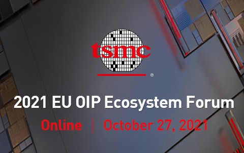
Our 2021 Open Innovation Platform® (OIP) Ecosystem Forum will take place online for Europe, North America, and China in October. The TSMC OIP Ecosystem Forum is a one-of-a-kind event that brings together the semiconductor design community and TSMC customers, providing an ideal platform for our customers to discuss with our ecosystem partners, about the latest technologies and design solutions for Mobile & Automotive, High-Performance Computing & 3DFabric, and IoT & RF applications. We look forward to seeing you at our Online event and sharing with you how our technologies and design ecosystem can help unleash the future of innovation.
As a responsible corporate citizen, TSMC strives to adapt to climate change and mitigate climate impact to protect our shared global environment. On September 16, TSMC marked the International Day for the Preservation of the Ozone Layer with a commitment to reach net zero emissions by 2050. The Company also published its Task Force on Climate-related Financial Disclosures (TCFD) Report, becoming a semiconductor industry frontrunner in climate disclosure while taking actions towards the Company’s environmental sustainability goals.
In a post-pandemic world, new digitalization trends are diversifying the demand for semiconductors. The era of digitalization will significantly grow the semiconductor industry and bring enormous opportunities to the industry in the next few years. At TSMC, we will continue to push technology forward to accelerate customers’ innovation and are committed to investing in R&D, science, and engineering, backed by a proven track record of providing the global industry with leading-edge technologies and services.