
This year, TSMC was excited to meeting our customers in person at the TSMC Technology Symposium for the first time since the pandemic began. We shared how technology continues to power digital transformation, changing the way we do business and learn from one another, be it online or in-person.
“How we connect with one another is about to dramatically change. How we relate to the world around us is also changing,” TSMC CEO Dr. C.C. Wei noted in his opening remarks. “AI, 5G, and soon-to-come 6G technologies are redefining things such as autonomous driving, digital healthcare, and climate change. As our world becomes smarter and more connected, we have to create even more intelligent edge devices.”
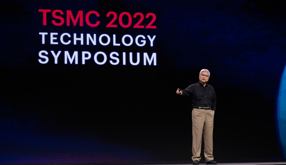
Event Keynote from TSMC CEO Dr. C.C. Wei
There are very real fundamental shifts in the semiconductor economic framework happening right now, and TSMC is dedicated to helping customers like you navigate this new world. With devices becoming smarter and more connected, there is an increasing need for more intelligent edge devices and massive computational power.
Even before the pandemic, companies started prioritizing resilience over cost in response to geo-political supply chain disruptions, with the pandemic accelerating this trend. As a result, we are seeing the industry shift to larger inventories designed to minimize disruption and have a growing preference for a more localized supply chain.
With these accelerated technology needs and challenging supply chain constraints, Dr. C.C. Wei reaffirmed TSMC’s commitment to being “everyone’s foundry” and supporting our customers’ sustained growth. Beyond the 12,000 products that TSMC has made together with customers using almost 300 different technologies in 2021, he highlighted how TSMC has shipped two million 5nm technology wafers to date that are being used in smartphones, 5G, AI, networking, and HPC applications.
“Collaboration is the fast lane to innovation. Thanks to our trusted relationship with TSMC, we are proud to announce the first test sample of a fully ASIL-D compliant 5nm SoC for automotive – it’s part of the S32 processor family and the first of its kind for the modern car,” said Kurt Sievers, President and Chief Executive Officer of NXP Semiconductors. “TSMC has been our partner of choice to drive advanced use cases forward in the mobile and edge computing market. We are very confident of our success together and are excited to leverage this fantastic opportunity of the secure, connected edge, going forward.”
Turning to 3nm progress, TSMC is seeing enthusiastic customer engagement for the technology, and development is on track with volume production set for the second half of 2022. And of course, Dr. Wei made a much-anticipated announcement about new transistor technology for TSMC’s N2 node.
“We have been working on nanosheet transistors for more than 15 years and have established very solid capabilities,” Dr. C.C. Wei added. “And we believe N2 is the right node to introduce nanosheet transistors to help customers stay competitive with a full-node speed and power gain.” Development of N2 is scheduled for 2025 volume production.
Additionally, Dr. Wei announced that last year’s N5A design supporting automotive applications such as ADAS and digital cockpits is on track to be automotive grade certified in the third quarter of this year.
“The most significant transition facing the automotive industry today is the demand for autonomous vehicles and associated customer experiences. As we undergo this transition, autonomous cars will become the ultimate edge device – generating and requiring more data and compute power than any other device that exists today,” said Herbert Diess, chairman of the board of management, Volkswagen AG. “As our cars evolve, our applications will need to become more advanced and complex, requiring close partnership with TSMC. Many devices within our cars still require traditional nodes – involving 50 to 90nm technology – but there will be a greater demand for cutting-edge silicon as our core architecture matures. The automotive company that integrates the most advanced silicon will be best equipped to build an autonomous vehicle that can navigate the harshest environments, while prioritizing both driver safety and customer experience.”
Dr. Wei also shared that TSMC more than doubled capital spending from under US$15 billion in 2019, to $30 billion in 2021, and $40-44 billion in 2022 as TSMC builds capacity for advanced technology, specialty technology, and 3DFabric to meet customer needs.
Along with this expanded capacity, green manufacturing continues to be of the utmost importance. TSMC has committed to reaching net zero emissions by 2050 and has set aggressive intermediate goals to stop emissions growth by 2025, and to reduce total emissions to the 2020 level by 2030. In terms of water use, TSMC will open its first off-site water reclamation plant in Tainan, Taiwan this year, reclaiming water at more than 1,800 gallons per minute.
Dr. C.C. Wei ended his keynote with a promise to all customers, “We’ll never compete with you, because we don’t produce any of our own products. We remain committed to building long-term strategic partnerships with each and every one of you.”
Advanced Technology
TSMC’s goal is to deliver industry-leading technological advancement at a steady and predictable pace, enhancing each technology node for additional performance, power, and density improvements while keeping design rules compatible to enable IP reuse.
| ● | Advanced Logic Technologies: TSMC’s Advanced industry-leading CMOS logic technologies enable product innovations, delivered in volume and on time to capture market opportunities. TSMC’s N7 and N6 product portfolio is expanding from smartphones, CPUs, GPUs, and XPUs, to RF and consumer applications. By the end of 2022, the accumulated number of product tape-outs will surpass 400. We’ve applied our experience from high-volume production not only to yield improvement, but also to performance, design rules, and chip density enhancements. Our N5 and N4 technologies are seeing continuous enhancement and we expect more than 150 product tape-outs by the end of this year. From N5 to N4X, we achieved 15% performance and 6% chip density improvements, while keeping design rules compatible to enable design reuse, more functionality, and better spec improvements. |
|---|---|
| ● | TSMC FinFlex™ Innovation Optimizes PPA Trade-offs: The new TSMC FinFlex™ architecture extends the product performance, power efficiency, and density envelope of the 3nm family of semiconductor technologies by allowing chip designers to choose the best option for each of the key functional blocks on the same die using the same design tools. These options include a 3-2 fin, 2-2 fin, and 2-1 fin configuration. with the following characteristics:
|
| ● | TSMC’s FinFlex™ architecture provides tremendous chip design advantage and flexibility, presenting a powerful platform for product innovation. 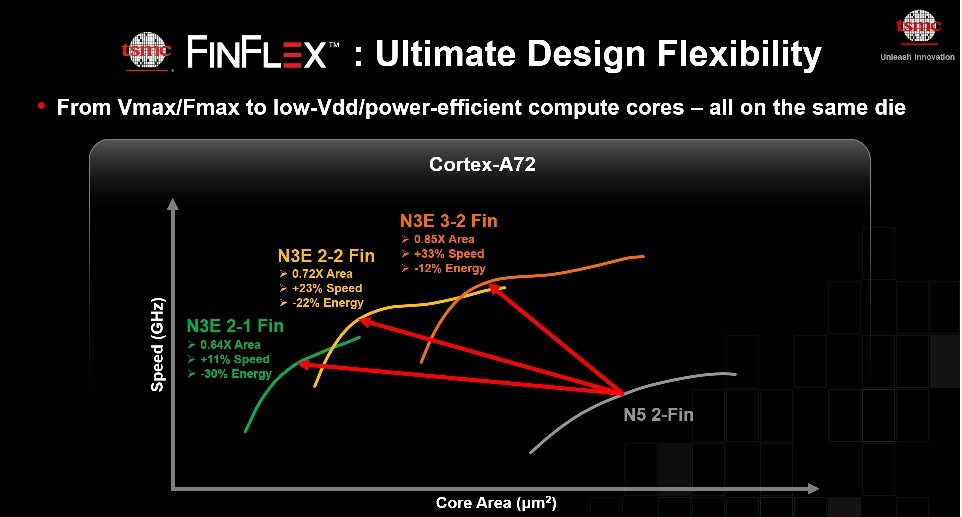 |
| ● | N2 and Nanosheet Transistors: For the N2 node, TSMC is adopting nanosheet transistors. With the help of the nanosheet transistors and Design-Technology Co-Optimization (DTCO), TSMC’s N2 offers full-node performance and power benefits. Owing to the extremely low Vdd performance of nano-sheet transistors, N2 improves performance by 15% with the same power at nominal Vdd and the advantage widens to 26% at a lower Vdd (0.55V). 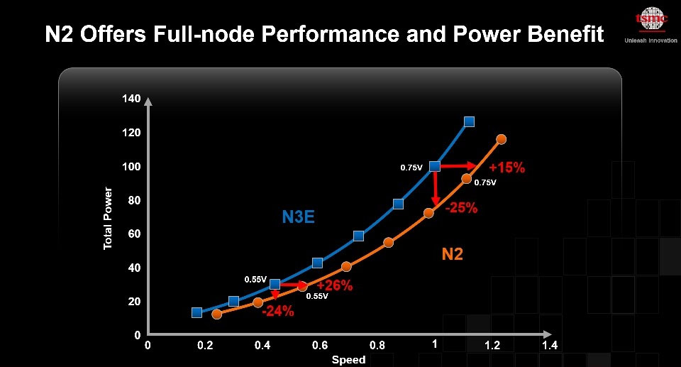 |
| ● | Technology Innovation Beyond N2: We are very optimistic about what lies ahead beyond N2, especially given the innovations emerging in novel transistor structures, new materials, continued scaling, and new conductor materials.
|
| ● | EUV Roadmap: To aggressively address pitch shrinking at key nodes, we began leveraging EUV scanners and multiple patterning at N7+. Looking ahead, TSMC will bring in High-NA EUV scanners in 2024 to develop the associated infrastructure and patterning solutions needed for customers to fuel innovation. |
Specialty Technologies
To support the semiconductor industry’s accelerated growth, TSMC strives to provide best-in-class specialty technologies for a broad spectrum of applications, including RF/connectivity, CMOS image sensing, MEMS, and power management. Our specialty technology investment has grown at about 64% CAGR in recent years, almost tripling the pace of our past investment. In the next few years, we expect more specialty capacity to become available.
| ● | Ultra-Low Power Technologies for IoT and Edge AI: Following TSMC N12e™, the next generation IoT platform that we’re announcing is N6e. This is based on our advanced 7nm technology and will bring three times greater logic density than N12e. It will serve as a part of TSMC’s Ultra-Low Power platform, a comprehensive portfolio of logic, RF, analog, embedded nonvolatile memory, and power management IC solutions aimed at applications in edge AI and the Internet of Things. |
|---|---|
| ● | Advanced RF Technologies for 5G & Connectivity: Advanced RF products require more high-performance and low-power computation capabilities. Our RF CMOS technology continues to deliver significant power and area reduction (-49% for power and -55% for area; comparing N6RF to N16 RF), while being able to fully offset the increased power/area demands of WiFi7. |
| ● | MCU / Embedded Nonvolatile Memories: TSMC has heavily invested and is executing on new embedded memories, such as MRAM and RRAM. Both technologies have already come to fruition, going into production at 22nm and 40nm nodes. We are now developing next-generation 12RRAM, which is expected to be ready by the end of 2023. 40RRAM production has been underway since the first quarter of 2022, with multiple customer product tape-outs being planned at both the 40nm and 22nm nodes. Our 22MRAM is currently in production for IoT/wearable applications, while 16MRAM qualification is planned for consumer applications in 2022 and automotive in 2023. |
| ● | CMOS Image Sensing: To process the data coming from more and more powerful sensors, the signal processor needs more computing power, and we anticipate that ISPs will move to 12nm FinFET processes. Going into the future, to achieve even more high-quality and intelligent sensing, we envision a multi-wafer stack solution, using TSMC’s wafer-on-wafer integration technology to put the signal processor right next to the sensor. |
| ● | Display: We are focusing on higher resolution and lower power consumption for many new applications, driven by 5G, AI, and AR/VR, merging display technology and silicon to enable new applications. TSMC’s leading µDisplay on silicon technology can deliver up to 10X pixel density to achieve the high resolution needed for a near-eye display like those used in AR and VR. |
Advanced Packaging
TSMC 3DFabric™ technologies enable ultimate system integration solutions, including TSMC’s leading silicon technologies, TSMC-SoIC™ chip stacking platform, as well as the Integrated Fan-Out (InFO) and Chip on Wafer on Substrate (CoWoS) advanced packaging platforms. TSMC’s advanced packaging capacity in 2022 will be 3X larger than it was in 2018. We will start SoIC silicon stacking manufacturing in 2022 and plan to expand the capacity to be over 20X in 2026.

| ● | New Fully Automated Fab: To provide that capacity, we now have the first fully automated fab for 3DFabric in Chunan, Taiwan that integrates advanced testing, SoIC, InFO, and CoWoS® operations together. This offers the best flexibility for customers to optimize their packaging by leveraging better cycle time and quality control. We will start SoIC production in the second half of 2022 and full 3DFabric operation in 2023. | ||||
|---|---|---|---|---|---|
| ● | 3DFabric Technology Developments: TSMC has also been working proactively with customers and DRAM partners to ensure robust high-bandwidth memory (HBM) and low-power DDR integration for CoWoS and InFO-PoP/InFO_B in HPC and mobile applications, respectively. Our SoIC Chip-on-Wafer (CoW) development starts from N7-on-N7 stacking that features 9μm bond pitch, followed by involving more advanced silicon nodes and finer bond pitches. We have already started production on N7-on-N7 SoIC-CoW process. As for SoIC Wafer-on-Wafer (WoW), TSMC delivered the world’s first N7 logic on deep trench capacitor (DTC) IPU product for AI applications. | ||||
| ● | Customer Collaboration:
|